- SK Hynix split-cell 5-bit flash increases SSD density without significantly reducing production complexity
- RAID-0-style parallelism in split-cell NAND boosts read speed dramatically
- Each half-cell reduces voltage stress, extending the endurance of the five-bit flash
The NAND flash industry continues to search for ways to increase storage density as demand rises from data centers, consumer devices, and AI tools.
Conventional scaling through additional 3D NAND layers has become increasingly complex, expensive, and difficult to manufacture consistently.
While four-bit QLC flash is already in commercial production, moving to five-bit PLC flash has remained impractical due to reliability and endurance problems tied to voltage-sensing limits.
How split-cell flash changes the equation
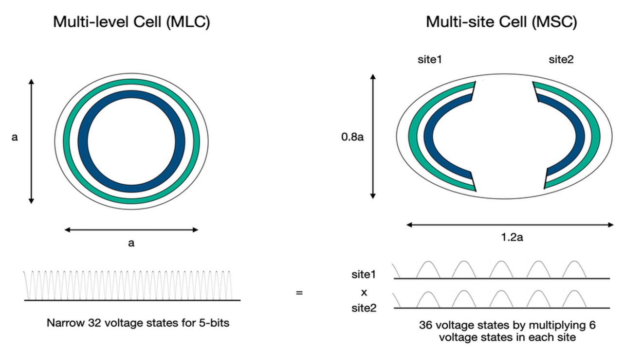
SK Hynix has introduced a different approach known as multi-site cell technology. Instead of forcing a single NAND cell to hold all 32 voltage states, the design splits the cell into two independent half-cells.
Each half stores six voltage states, which combine to represent a five-bit value. This design reduces voltage crowding while maintaining overall bit density.
The two half-cells operate in parallel as a single logical unit, resembling how RAID-0 spreads data across hard drives to increase throughput.
In this case, voltage states combine during access rather than being striped across separate devices.
The physical cell shape is elliptical rather than circular, which allows space for an insulating wall between the halves and separate bit line connections.
SK Hynix says wider voltage gaps within each half-cell reduce electron leakage and shorten programming time.
The two halves are read simultaneously, which the company claims delivers faster read speeds compared with conventional PLC designs.
This method also improves endurance, as lower voltage stress reduces wear on the cell.
SK Hynix demonstrated working wafers at the 2025 IEDM conference, signaling that the concept extends beyond simulation.
The split-cell approach requires additional semiconductor process steps, including cell division and gap filling, which adds cost and complexity.
While SK Hynix is evaluating manufacturability, other flash makers, including Samsung, Micron, Kioxia, and Sandisk, are expected to study similar ideas.
The concept does not promise cheaper SSDs, only denser ones, and it does not remove the role of hard drives in large-scale capacity storage.
If manufacturers can produce multi-site cells at scale, PLC flash may finally become viable without the severe drawbacks seen in earlier designs.
Via Blocks & Files
Follow TechRadar on Google News and add us as a preferred source to get our expert news, reviews, and opinion in your feeds. Make sure to click the Follow button!
And of course you can also follow TechRadar on TikTok for news, reviews, unboxings in video form, and get regular updates from us on WhatsApp too.
Source: TechRadar